bence burada görsellerden kaynaklı bir algı hatası var. görsellere göre birbirine seri bağlı 2 diyot varmış gibi görünüyor. çıkan sonuç saturasyon halindeki bir bjt transistörde emiter-kolektör arası iç direnç çok düşük olurken. base emiter veya base collectör arası direnç değişmiyor.
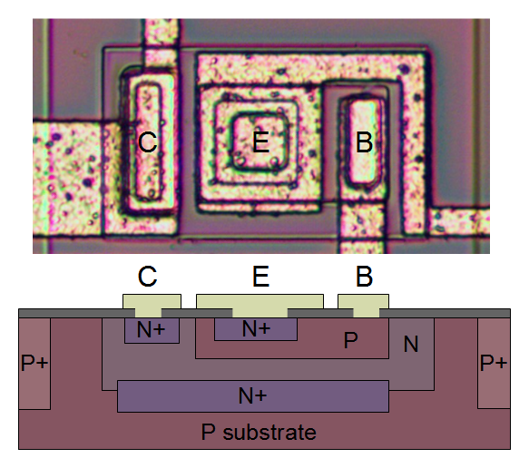
silikon seviyesinde bjt transistörü anlatan bir video:
ayrıca şöyle bir yanıt da var:
Why does only a small current flow out of the base in an NPN transistor and the majority flow from emitter to collector?
In the case of an NPN transistor, the base is positive with respect to the emitter; and lets say the emitter is actually connected directly to ground for purposes of this example. as you begin to conduct current between the base and emitter, electrons leave the emitter and move into the base. These electrons that are now in the base can go two places. Out the base lead or jump between the base and collector. As we know, the there is a positive charge in the base between the base and collector, so what’s the electron going to do. Is it going to fill a hole in one of those positive charges, or is it going to go out the base lead. Well as it turns out and as a function of the design, about 99 out of 100 electrons end up filling the hole. Once that hole is filled, an electron can move from the collector where it was part of the depletion region between the base and collector and go out to the source through the collector lead. That first electron by the way finds it’s way into the collector. Hope that’s all kind of clear.
What you’re looking at is an electron that just entered the base material, and finds itself in a really long hall with 100 doors 99 of which lead to the collector and the one at the very end of the hall leads to the base. Don’t forget about the attraction of the positive charge and electron negative charge. What’s the likely hood the electron’s going to end up going out the base lead? That one electron that doesn’t get sucked into any one of the positive charges leading to the collector will leave through the base lead.
It’s my understanding the thicker the base material and the more narrow the channel through which the electrons can travel through that base material results in a smaller current Gain. Why? Given the shorter distance to travel to the base lead and the distance the electron has to travel to get to the collector, the odds increase that the electron will make it to the base lead.

 fakat mosfeti düşünsek doğru gibi bu yazdıklarım.